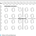
An FPGA is a semiconductor device on which the function can be defined after manufacturing. An FPGA enables you to program product features and functions, adapt to new standards, and reconfigure hardware for specific applications even after the product has been installed in the field — hence the term field programmable. A field-programmable gate array (FPGA) is an integrated circuit designed to be configured by a customer or a designer after manufacturing – hence the term “field-programmable”.
The FPGA configuration is generally specified using a hardware description language (HDL), similar to that used for an application-specific integrated circuit (ASIC). Circuit diagrams were previously used to specify the configuration, but this is increasingly rare due to the advent of electronic design automation tools
ASIC stands for Application Specific Integrated Circuit. An ASIC is similar in theory to an FPGA, with the exception that it is fabricated as a custom circuit. This means that – unlike FPGAs – it is not reprogrammable, so you had better get it right the first time! Since ASICs are custom circuits, they are very fast and use less power than an FPGA. This can be critical in power-sensitive applications such as cell phones, mp3 players, and other battery-operated devices.
The biggest drawback to an ASIC is cost. To get a company to build an ASIC for you will cost hundreds of thousands of dollars as an initial investment!
FPGAs contain an array of programmable logic blocks, and a hierarchy of “reconfigurable interconnects” that allow the blocks to be “wired together”, like many logic gates that can be inter-wired in different configurations. Logic blocks can be configured to perform complex combinational functions, or merely simple logic gates like AND and XOR. In most FPGAs, logic blocks also include memory elements, which may be simple flip-flops or more complete blocks of memory. Many FPGAs can be reprogrammed to implement different logic functions, allowing flexible reconfigurable computing as performed in computer software. FPGAs have a remarkable role in the embedded system development due to capability to…
-
- start system software (SW) development simultaneously with hardware (HW)
- enable system performance simulations at very early phase of the development
- allow various system partitioning (SW and HW) trials and iterations before final freezing of the system architecture
As you may already know, FPGA essentially is a huge array of gates that can be programmed and reconfigured any time anywhere. “Huge array of gates” is an oversimplified description of FPGA. FPGA is indeed much more complex than a simple array of gates. In less technical terms, an FPGA allows you flexibility in your designs and is a way to change how parts of a system work without introducing a large amount of cost and risk of delays into the design schedule.
A simple example is a rear-view camera designed for a car. If your camera system takes 250 milliseconds from the time the image sensor sees the image until the image frame actually appears on the display, and a change in government regulations requires that this delay or latency be no more than 100 milliseconds, you could find ways to adjust the image signal processing pipeline in an FPGA to comply with the new latency requirements. This would be almost impossible to do with a microprocessor-based system. In this example, a company can gain a big advantage using an FPGA because it doesn’t have to redesign parts or buy all new processors.
In the early days, FPGA circuits were very large and you couldn’t fit many onto a single chip. All a designer could do was build an interface with an FPGA and customers could re-program that interface to do something different (for example, changing an interface that operates on a keyboard input to one that handles input from a touchscreen device).
Soon, however, designers realized they could build entire sub-systems out of FPGAs, which meant designers were no longer restricted to only using ASICs to implement these subsystems. Because circuit components keep getting smaller and smaller, designers can put many more devices on the same chip — allowing for more sophisticated functionality and faster arithmetic, which in turn leads to faster computation and less power consumption.
Modern FPGAs consist of mixes of configurable static random access memory (SRAM), high-speed input/output pins (I/Os), logic blocks, and routing. More specifically, an FPGA contains programmable logic elements called, naturally, logic elements (LEs), as well as a hierarchy of reconfigurable intercon-nects that allow the LEs to be physically connected to one another.
You can configure LEs to do complex functions or simply perform basic logic gates, such as AND and OR. Most FPGAs also contain memory blocks.
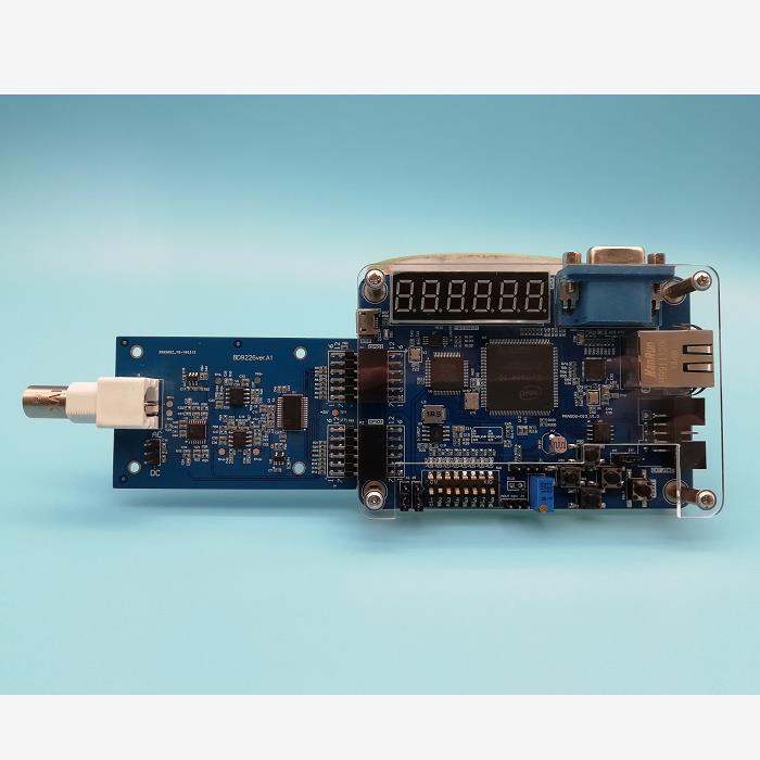
FPGA boards, or Field-Programmable Gate Array boards, are basically integrated circuits which are, as its name suggests, programmable on the field. In other words, the end-user or the secondary manufacturer can program the board to their liking; however they wish it to be configured.
FPGA boards are configured with the use of HDL or Hardware Description Language, however, although very rare, circuit diagrams have been used in the past. FPGAs have components called logic blocks, which make the former what they are: reconfigurable.
These logic blocks are somewhat the opposite of logic gates, in a sense that the latter are manufactured with specific functions while the former are to be programmed after manufacturing, before they can be used. Along with these logic blocks are a group of interconnects that are also reconfigurable.
