JTAG (Joint Test Action Group) is a interface used for debugging and programming the devices like micro controllers and CPLDs or FPGAs.
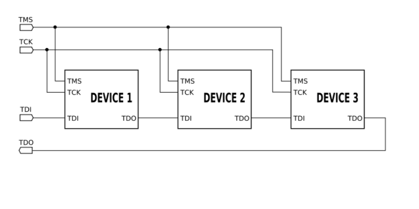
Joint Test Action Group (JTAG) is the common name used for a debugging, programming, and testing interface typically found on microcontrollers, ASICs, and FPGAs. It enables all components with this interface to be tested, programmed, and/or debugged using a single connector on a PC board which can daisy chain them together.
JTAG is the name of the group that defined the IEEE 1149.1 standard. This standard defines the Test Access Port (TAP) controller logic used in processors with JTAG interfaces.
Required below pins –
TMS -Test Mode Select
TCK – Test Clock Input
TDI – Test Data Input
TDO – Test Data Output
TRST – Test Reset (optional)
- TMS – selects the device under test
- TCK – clocks data into TDI
- TDI – the test or programming data input, cascaded through all JTAG compliant devices in the system
- TDO – the resulting output
- TRST – Test reset
JTAG Connector
There is no standard JTAG connector or pinout, so suppliers are able to define their own. This unique interface enables you to debug the hardware easily in real time (i.e. emulate). It can control directly the clock cycles provided to the micro controller through software. Therefore you can put hardware breakpoints in your code execution. You can start, pause, stop the execution of the code in the hardware as you want. For simplicity, one may assume the following hardware.
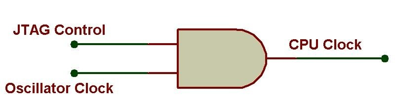
Whenever JTAG control is set to ‘1’, oscillator clock will be connected to CPU, else CPU will not receive clock and cannot execute any instruction. This way, you can control the execution of instructions in hardware.
For programming the CPLDs/FPGAs, JTAG uses parallel port of the computer. However, you can program your micro controllers through USB port.
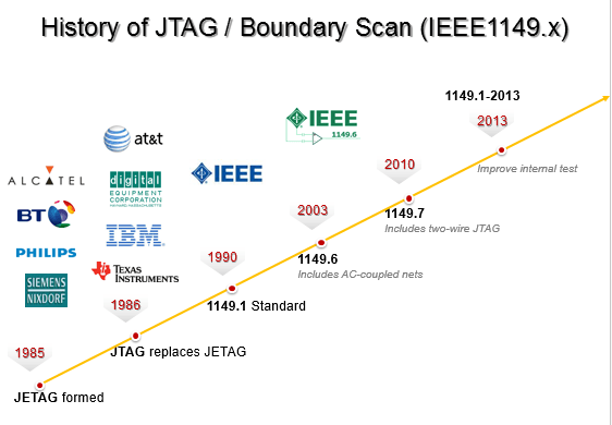
JTAG is a common hardware interface that provides your computer with a way to communicate directly with the chips on a board. It was originally developed by a consortium, the Joint (European) Test Access Group, in the mid-80s to address the increasing difficulty of testing printed circuit boards (PCBs). JTAG has been in widespread use ever since it was included in the Intel 80486 processor in 1990 and codified as IEEE 1491 that same year. Today JTAG is used for debugging, programming and testing on virtually ALL embedded devices.
Boundary Scanning
With the invention of integrated circuits came the need to test physical interconnects. That is: test whether “Point A” on a circuit board correctly connects to “Point C”. As industry drove toward higher density interconnects and finer pitch (i.e. smaller) components, a standardized way of testing integrated circuits (or “chips”) was needed. By embedding the test logic within the IC itself and limiting the physical interface to just a few signals, JTAG/boundary-scan presented an elegant solution to testing, debugging, and diagnosing modern electronic systems. Simply stated, boundary Scanning allows you to read and write individual bits, on individual pins, of the individual chips on a board. This ability to read and write 1’s and 0’s directly onto the pins is extremely powerful, but widely misunderstood.
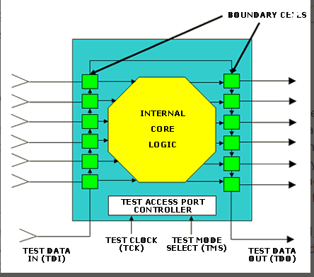
The JTAG interface gives manufacturers a way to test the physical connections between pins on a chip. When electrical engineers talk about using JTAG to “debug” a chip, they are talking about something very different than traditional software debugging. They are talking about making sure pin A on chip A is physically connected to pin B on chip B, and that all those pins are functioning correctly. Since JTAG gives you direct hardware access to a device, it’s also a fantastic tool for security research.
JTAG Fundamentals
Before we go into using JTAG to actually hack something, let’s review the JTAG fundamentals.
4 Pins, Plus 1
The official JTAG standard requires 4 standard pins (or signals), and defines an optional 5th. These signals, and the small bit of silicon logic that connects and controls them, are collectively referred to as the Test Access Port, or TAP controller.
One of the most confusing thing about learning to get hands-on with JTAG is how much partial and disinformation there is about it. Manufacturers’ websites tell you the “theory” of how it works, but leave you longing for more information about “how to get started”. To further confuse things there are other factors:
- Buzzword: It is a infosec buzzword, everyone talks about it but few really share actionable info
- Loaded Word: JTAG has come to mean many things to many people. For example, in the gamer community “JTAG” means a hardware modification for a console that allows playing pirated games or loading homebrew content (i.e. “a jtagged XBox”). This makes it difficult to search for useful information.
- Vernacular Overlap: As mentioned above, when an Electrical Engineer says “debug” he means: “Are the pins in the right place? Is there enough power? Is the logic of the circuit correct?” When a Software Engineer says “debug” he thinks of GDB or WinDBG. JTAG is designed for the former, not the latter.
- Misunderstanding: As software developers the closest similarity to JTAG is maybe Kernel debugging via a debug cable (USB, Parallel, or Serial). But this is a dangerous comparison, because even on the “debugee” (in that scenario) there is software code executing on the remote system handling the translation of commands arriving on the debug cable. The JTAG state machine implemented entirely in hardware on the target.
Here is what JTAG is. In it’s most fundamental. The JTAG specification 1149.1 requires these five signals:
- TCK: Test Clock
- The drummer, or metronome that dictates the speed of the TAP controller. Voltage on this pin simply pulses up and down in a rhythmic, steady beat. On every “beat” of the clock, the TAP controller takes a single action. The actual clock speed is not specified in the JTAG standard. The TAP controller accepts its speed from the outside device controlling JTAG.
- TMS: Test Mode Select
- Voltages on the Mode Select pin control what action JTAG takes. By manipulating the voltage on this pin, you tell JTAG what you want it to do.
- TDI: Test Data-In
- The pin that feeds data into the chip. The JTAG standard does not define protocols for communication over this pin. That is left up to the manufacturer. As far as JTAG is concerned, this pin is simply an ingress method for 1s and 0s to get into the chip. What the chip does with them is irrelevant to JTAG.
- TDO: Test Data-Out
- The pin for data coming out of the chip. Like the Data-In pin, communication protocols are not defined by JTAG.
- TRST: Test Reset (Optional)
- This optional signal is used to reset JTAG to a known good state, we’ll explain why this is optional in a few paragraphs.
There are two types of registers associated with boundary scan. Each compliant device has one instruction register and two or more data registers.
Instruction Register – the instruction register holds the current instruction. Its content is used by the TAP controller to decide what to do with signals that are received. Most commonly, the content of the instruction register will define to which of the data registers signals should be passed.
Data Registers – there are three primary data registers, the Boundary Scan Register (BSR), the BYPASS register and the IDCODES register. Other data registers may be present, but they are not required as part of the JTAG standard.
- BSR – this is the main testing data register. It is used to move data to and from the I/O pins of a device.
- BYPASS – this is a single-bit register that passes information from TDI to TDO. It allows other devices in a circuit to be tested with minimal overhead.
- IDCODES – this register contains the ID code and revision number for the device. This information allows the device to be linked to its Boundary Scan Description Language (BSDL) file. The file contains details of the Boundary Scan configuration for the device.
How JTAG / boundary scan is used to test a board
Boundary scan cells (see above) can operate in two modes. In their functional mode they have no effect on the operation of the device – this is the mode in which they operate when the board is running normally. In their test mode they disconnect the functional core of the device from the pins. By putting boundary scan cells into test mode they can be used to control the values being driven from an enabled device onto a net and also be used to monitor the value of that net.
Disconnecting the control of the pins from the functionality of the enabled device makes boundary scan test development significantly easier than traditional functional test as no device configuration or booting is required to use the pins. By providing a mechanism to control and monitor all the enabled signals on a device from a four-pin TAP, JTAG significantly reduces the physical access required to test a board.
There are two main ways that this boundary scan capability can be used to test a board. The first way, connection testing (see next section) gives good test coverage, particularly for short circuit faults. It is based purely on the JTAG device capabilities, the connections and nets on the board and – in the case of XJTAG – the logic functionality on a board. The second way extends this coverage by using the JTAG enabled devices on a board to communicate with non-JTAG peripheral devices such as DDR RAM and flash.
For more Jtag information, please check https://fraserinnovations.com/jtag/
FPGA Board with Jtag Embeded
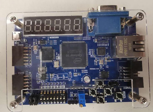
The advantage of FPGA beginner study board:
- Beginner FPGA study board, cheaper but fully functional. cellphone sized. ( < 100 USD )
- power supply and download at the same time, no extra power supply and no extra data transfer line needed
- Small volume and light and can be put into your pocket. size: 10cm X 7 cm.
- Unique function: can be a study board as well a multifunctional JTAG downloader.
- We use newest version Intel FPGA within two years and you can always keep in the front of FPGA industry.
Altera FPGA Study Board Hardware Resources:
- 6 seven_seg_r
- VGA Video Interface × 1
- 1G Ethernet Interface × 1
- I2C EEPROM × 1
- DIP Switch × 8
- Controllable LED light × 8
- Photoresistance × 1
- Thermistor × 1
- Adjustable Varistor × 1
- Buttons × 4
- GPIO Interface × 2
- Micro usb Interface(Power Supply and downlaod ) × 1
- SPI Communication Interface × 1
- AD/DA Conversion chip × 1
- JTAG Download Interface × 1
- FLASH 32Mbit × 1